
“Two-dimensional materials, such as graphene, possess unique properties that can be utilized to create various new electronic and optoelectronic devices. However, the development of 2D devices has been constrained by the limitations of effective large-area transfer processes. One important method involves stacking 2D materials through controlled van der Waals interactions, allowing for the synthesis of novel materials with high degrees of freedom. This method enables scientists to create materials with different compositions and twist angles, opening up possibilities for various practical applications. However, existing transfer methods often degrade the electronic performance and quality of 2D materials, affecting the final device performance and increasing process time and production costs.
To address these issues, researchers have tried various transfer methods. The most common approach involves using thin support layers, such as polymethyl methacrylate (PMMA), polystyrene, paraffin, rosin, and volatile molecular-PMMA composites. However, transferring through thin support layers typically leaves organic residues on the surface of 2D materials and limits the choice of target substrates. Additionally, the transfer process based on thin support layers tends to produce wrinkles and cracks and is challenging to scale up to the large areas required for industrial processing.
The team led by Atsushi Yasui and Professor Hiroki Ago at the Global Innovation Center of Kyushu University in Japan has proposed a new transfer method using UV-controllable adhesive tapes to transfer graphene and other 2D materials. This method can produce large-area, high-quality, transferred monolayer graphene films, with a transfer yield of over 99% and a room-temperature carrier mobility exceeding 5000 cm²/Vs. This method is also applicable to other 2D materials, such as bilayer graphene (BLG) and transition metal dichalcogenides (TMDs), and allows for adjustment of the adhesive layer composition and transfer procedure. The emergence of this method provides a new avenue for large-scale transfer of 2D materials, offering user-friendly, simple, scalable characteristics that meet industrial needs. The related research findings were published in “Nature Electronics” under the title “Ready-to-transfer two-dimensional materials using tunable adhesive force tapes.”
To address the challenge of large-area transfer of graphene, researchers have developed a functional adhesive tape with UV-controllable adhesive force. In the experiment, the tape was first placed over high-quality monolayer graphene grown on Cu(111) film, and the adhesive layer was hardened using UV light. Through an electrochemical delamination and cleaning process, the graphene was transferred from the Cu substrate to a SiO2/Si substrate. Figure 1a shows this transfer process. Figure 1b presents an optical micrograph of the transferred graphene sheet, indicating that UV light is crucial for the uniform transfer of graphene. Figures 1c and 1d show optical images of the Cu surface before and after transfer and the SiO2 surface, confirming the successful transfer of graphene to the SiO2 surface. Analysis of ten transfer batches, shown in Figure 1e, demonstrates a high yield of graphene transfer. Figure 1f displays the Raman spectrum of the transferred graphene, proving its high quality. Figure 1g maps the ID/IG intensity ratio of the graphene, indicating almost no structural defects. Figure 1h shows the electron mobility histogram of field-effect transistors made from the transferred graphene. Finally, Figure 1i illustrates the potential of this method in large-area transfer and stacking of graphene by showing a trilayer graphene sheet stacked using the method.
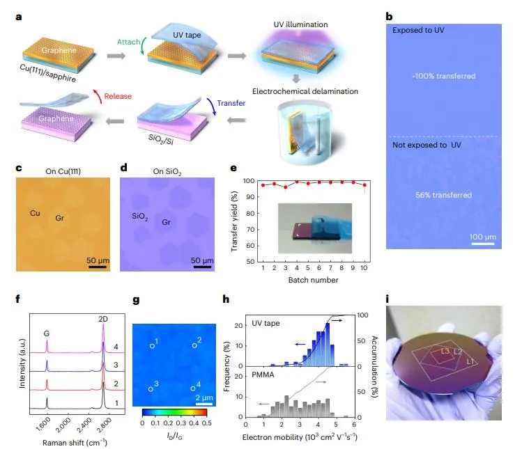
Figure 1. UV adhesive tape-assisted transfer of monolayer graphene and its characterization.
To compare the UV adhesive tape method with other transfer methods, the authors compared it with the most widely used PMMA film and TRT used for large-area graphene transfer in Figure 2. The surface of graphene transferred using the UV adhesive tape (Figure 2a) is cleaner and has a lower fracture density compared to the PMMA-transferred graphene (Figure 2b). TRT transfer caused damage to the graphene and left many adhesive residues (Figure 2c). AFM images show that the surface of the graphene transferred with the UV adhesive tape has almost no impurities and lower surface roughness (Figure 2d). In comparison, PMMA transfer caused some fractures in the graphene (Figure 2e), while TRT left a high density of adhesive residues (Figure 2f). The surface roughness distribution of graphene transferred with the UV adhesive tape is more concentrated (Figure 2g). X-ray photoelectron spectroscopy analysis shows that the graphene surface after UV adhesive tape transfer has almost no residues, whereas the surfaces of graphene transferred with PMMA and TRT show significant contamination and residues. Therefore, the graphene produced by the UV adhesive tape transfer method has higher quality and a cleaner surface.
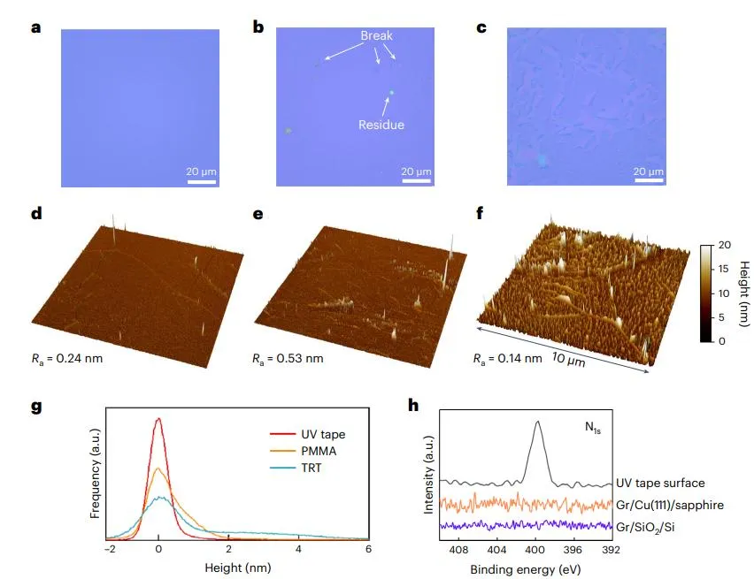
Figure 2. Comparison with other transfer methods.
Figure 3 shows the experimental results of using UV adhesive tape to transfer other two-dimensional (2D) materials and fabricate stacked heterostructures. The authors successfully transferred monolayer MoS2 and other CVD-grown transition metal dichalcogenides (TMDs) from their growth substrates to SiO2/Si substrates, demonstrating the effectiveness of the tape transfer method. MoS2 on SiO2 exhibited high-quality n-type semiconductor behavior, with an electron mobility of up to 23 cm²/V·s, and its surface was cleaner compared to MoS2 transferred using PMMA. The authors also successfully fabricated stacked heterostructures of MoS2/WS2 and confirmed the strong interaction between the 2D materials through Raman spectroscopy and photoluminescence spectroscopy. Additionally, the authors applied the UV adhesive tape method to transfer multilayer hBN and graphene, creating graphene-hBN stacked structures. Raman spectroscopy indicated that the 2D band full width at half maximum (FWHM) of graphene in the graphene-hBN heterostructure was the narrowest, suggesting the structure’s effectiveness in screening out the effects of the SiO2 substrate and surface gas adsorption. Overall, these experimental results indicate that the UV adhesive tape transfer method has broad application prospects in the preparation and study of stacked structures of 2D materials.
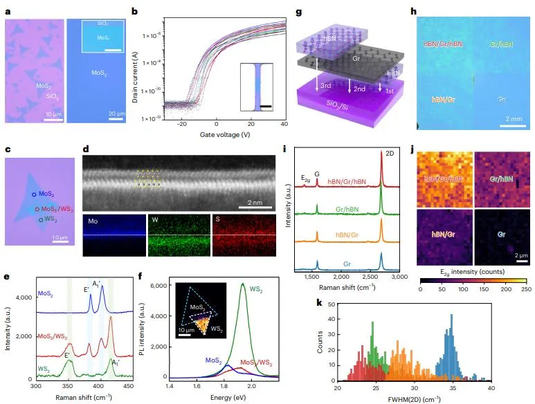
Figure 3. Transfer of other 2D materials and preparation of stacked heterostructures.
Figure 4 illustrates a cutting and transfer method for pattern transfer of 2D devices. In practical device applications using 2D materials, such as photodetectors, the total active area of 2D materials needed for a single wafer is usually very small. Thus, when transferring a large piece of 2D material, most of the area needs to be removed through photolithography and etching processes, leaving small channels in pre-designed positions. To validate this concept, the UV adhesive tape carrying monolayer MoS2 was cut into small pieces (Figures 4a-c). After placing each tape/MoS2 piece onto a SiO2 substrate using a guide, the tape was removed by heating the SiO2 substrate to 80°C. Due to its mechanical toughness, the small-sized UV adhesive tape is easier to handle compared to previously used PMMA. This ease of handling in the UV adhesive tape transfer process makes it an ideal choice for automated processing, allowing for better transfer accuracy, quality, and yield.
Figures 4d and 4e show the monolayer MoS2 patterns prepared on a 4-inch SiO2 wafer. A shadow mask was used to evaporate metal electrodes for fabricating MoS2 field-effect transistors (Figure 4f). The patterned MoS2 devices exhibited n-type carrier transfer and showed significant photoconductive response to visible light (432 nm wavelength) (Figure 4g). The cutting and transfer process described here can significantly reduce the area of 2D materials needed, thereby lowering production costs associated with synthesizing 2D materials at the wafer scale. Using large-area monolayer graphene grown on Cu(111)/sapphire, the authors were able to cut and stack graphene sheets and control the twist angle, as shown in Figure 4h. Figure 4i shows a photograph of an artificial bilayer graphene (BLG) stacked using oriented monolayer graphene, where four small pieces and one large piece of monolayer graphene were stacked using the UV adhesive tape. The tape’s toughness allowed the authors to cut and handle small pieces of graphene while maintaining their initial angles, thus defining the twist angle. Raman spectra taken on different stacks (Figure 4j) demonstrated characteristic features corresponding to the given twist angles, supporting the authors’ method’s excellent control over twist angles.
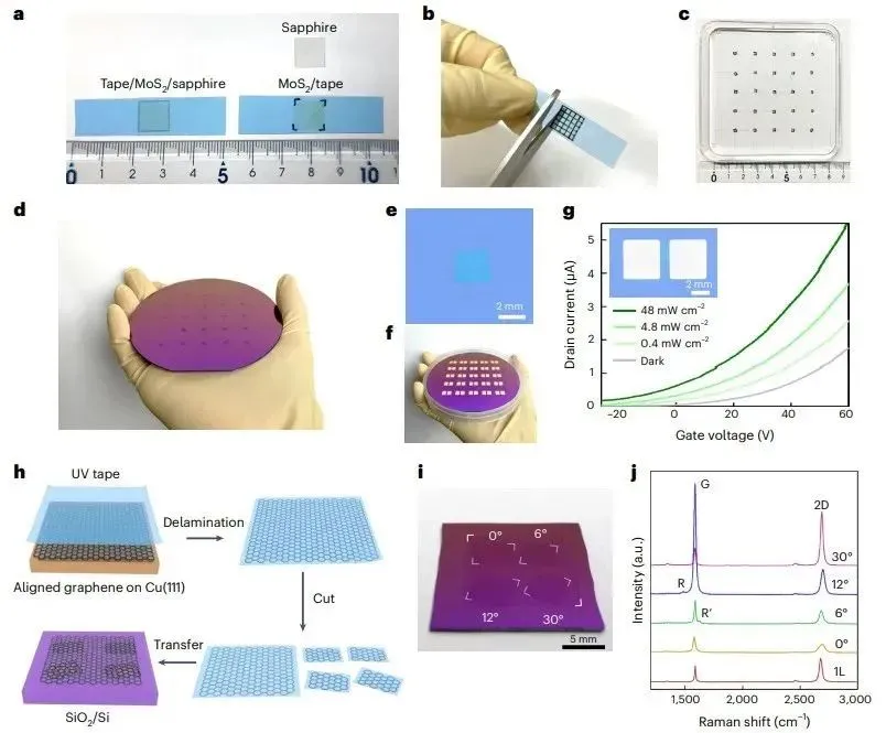
Figure 4. The process of cutting and transferring MoS2 and graphene.
Figure 5 showcases the versatility of the 2D tape and its applications in various fields. In Figure 5a, a schematic of a 2D tape library is shown, which can be used for large-scale transfer of different 2D materials. To demonstrate the broad applicability and effectiveness of the UV adhesive tape transfer method, the authors transferred graphene and TMDs onto various substrates. Monolayer graphene was transferred onto a ceramic surface, showing that the UV adhesive tape allowed the transfer onto curved surfaces of non-ideal materials (Figure 5b). The transfer with UV adhesive tape is gentle enough to allow the transfer of 2D materials onto suspended regions, as demonstrated by transferring graphene onto fine grids for transmission electron microscopy and SiO2 substrates with micron-wide grooves (Figures 5c-e). Notably, after contacting the 2D material on the target substrate, the tape can be peeled off by heating at moderate to low temperatures. Furthermore, this process does not require organic solvents to remove the support layer. This low-temperature and solvent-free release process allowed the authors to transfer graphene and MoS2 onto paper and plastic glasses.
In addition, the authors could create heterostructures of graphene and MoS2 on flexible polyethylene naphthalate (PEN) substrates (Figures 5f-h). Overall, the versatility of the UV adhesive tape in transferring 2D materials onto various surfaces has been demonstrated, even under non-ideal conditions. This flexibility makes it a reliable choice for various applications. Using monolayer graphene transferred onto a PEN substrate, the authors fabricated terahertz (THz) and infrared (IR) optical sensors. The transferred graphene was used to monitor the voltage induced by THz waves passing through a metal blade and paper envelope. THz mapping clearly showed the presence of the blade, characterized by a lower transmitted THz response due to the reflection of THz waves.
The researchers also detected the edges of the paper due to the scattering of THz waves. Graphene on the PEN substrate was also used for IR imaging of a match and two pieces of paper stored inside a black polyethylene bag. As shown in Figure 5m, the materials inside the bag were clearly identified by the graphene sensor due to their higher absorption rate of IR light.
Finally, the authors demonstrated a thermal imaging device made using graphene patterns on a four-inch PEN substrate. The monolayer graphene supported by UV adhesive tape was cut into 25 square pieces. Each piece of graphene was transferred to predefined locations on the transparent PEN substrate to create a 5×5 device array connected to Ti and Au electrodes. The authors successfully used the graphene device array to detect far-infrared light emitted from a soldering iron rod (Figure 5p). Even when an opaque sheet was placed between the soldering iron rod and the graphene, the authors could still detect infrared light using the graphene sensors.
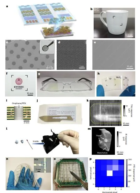
Figure 5. Versatility of the 2D tape and its applications.
/ Summary and Outlook /
This paper presents a method for transferring 2D materials using UV-controlled adhesive force tape, offering new possibilities for practical applications of 2D materials in electronics. By optimizing the tape composition, it is possible to achieve clean and efficient transfer of various types of 2D materials, avoiding impurities and defects that may arise from conventional transfer methods. Moreover, this method can be used to prepare vertical stacks of multiple 2D materials, allowing precise control of stacking angles. With simplified operation and low-temperature, solvent-free release steps, 2D materials can be easily transferred to various target substrates, including curved and complex surface structures. This innovative method provides a more convenient and efficient pathway for the large-scale application of 2D materials, opening up new possibilities for their use in electronics, optics, and sensors.
Source: Changshi New Energy