
What is the Graphene?
Graphene, a single layer of carbon atoms arranged in a two-dimensional honeycomb lattice, has been heralded as a revolutionary material since its isolation in 2004. Due to its remarkable electrical, thermal, and mechanical properties, it has sparked significant interest in various high-tech fields, including electronics, photonics, sensors, and energy storage. One of the key developments in graphene’s journey toward commercialization is the creation of graphene wafers, which serve as a foundation for integrating graphene into semiconductor manufacturing processes and other industrial applications.
1. Graphene Wafer Structure and Properties

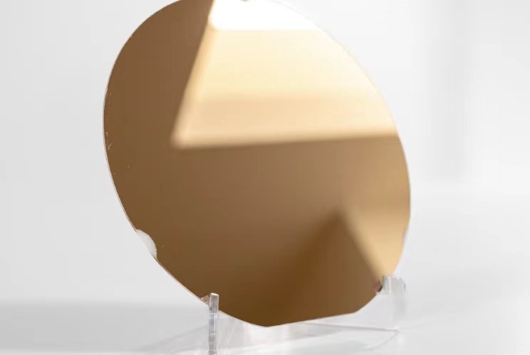
A graphene wafer consists of a thin layer of graphene deposited or synthesized on a substrate, such as silicon, silicon carbide (SiC), or copper. The process to create such a wafer involves either mechanical exfoliation (peeling off graphene layers from graphite), chemical vapor deposition (CVD), or epitaxial growth on SiC wafers.
Graphene wafers combine the exceptional properties of graphene with the robustness and scalability of wafer-based processing. The most notable properties of graphene include:
- High Electrical Conductivity: Graphene’s electron mobility at room temperature is approximately 200,000 cm²/V·s, making it far superior to traditional materials like silicon.
- Exceptional Strength: With a tensile strength of around 130 GPa, graphene is about 200 times stronger than steel, despite being extremely lightweight.
- High Thermal Conductivity: Graphene has a thermal conductivity of around 5000 W/m·K, making it ideal for heat dissipation applications in electronics.
- Transparency: Despite its conductive properties, graphene is nearly transparent, absorbing only 2.3% of visible light, making it suitable for optoelectronic applications.
2. Manufacturing Techniques for Graphene Wafers
Several techniques are used to produce graphene wafers, with each having its own advantages depending on the application and desired quality of the graphene:
A. Chemical Vapor Deposition (CVD)
This is the most common method for producing large-area graphene films. In CVD, a carbon-containing gas (like methane) is introduced into a chamber containing a heated substrate, such as copper foil. The carbon atoms from the gas decompose and deposit onto the substrate, forming a thin graphene layer. Once deposited, the graphene layer can be transferred onto other substrates, such as silicon wafers, for further processing.
- Advantages: CVD produces high-quality, large-area graphene films that are scalable for industrial production.
- Challenges: The transfer process from copper to silicon can introduce defects, and controlling the number of layers precisely can be challenging.
B. Epitaxial Growth on Silicon Carbide (SiC)
Epitaxial graphene is grown directly on the surface of a SiC wafer by heating the wafer in a vacuum, causing the silicon atoms to evaporate and leaving behind a layer of carbon atoms in the form of graphene.
- Advantages: This method creates high-quality, large-scale graphene with excellent electrical properties, and it doesn’t require a transfer step.
- Challenges: SiC wafers are expensive, and the process is complex.
C. Mechanical Exfoliation
While not suitable for large-scale production, mechanical exfoliation (also known as the “Scotch tape method”) was the original technique used to isolate graphene. It involves physically peeling thin layers of graphene from bulk graphite using adhesive tape.
- Advantages: This method can produce extremely high-quality graphene.
- Challenges: It’s not scalable for industrial applications due to its labor-intensive nature.
3. Applications of Graphene Wafers
Graphene wafers have the potential to revolutionize a variety of industries due to their superior properties. Some of the key applications include:
A. High-Frequency Electronics
Graphene’s high electron mobility makes it an ideal candidate for developing next-generation transistors, such as field-effect transistors (FETs) that can operate at higher frequencies than traditional silicon-based devices. Graphene wafers integrated with semiconductor technologies could enable ultra-fast electronic devices with lower power consumption.
B. Flexible Electronics
Graphene’s mechanical flexibility and transparency make it suitable for flexible electronic devices, such as foldable phones, wearable sensors, and flexible displays. Using graphene wafers, these devices could maintain excellent electrical performance while being bent or folded.
C. Optoelectronics
Graphene’s optical properties, such as its ability to absorb light across a wide range of wavelengths, make it useful for photodetectors and transparent conductive electrodes. Graphene wafers are being investigated for use in solar cells, light-emitting diodes (LEDs), and other optoelectronic devices, where they can improve efficiency and reduce energy consumption.
D. Quantum Computing
Graphene’s unique electronic properties, especially its ability to behave as a conductor or an insulator depending on external conditions, make it an exciting material for quantum computing. Graphene wafers could be used to create novel qubits and other components necessary for the development of quantum computers.
E. Biosensors
Due to graphene’s high surface area and sensitivity to environmental changes, graphene wafers are ideal for biosensing applications. They can be used to detect minute quantities of biological or chemical substances, leading to the development of highly sensitive medical diagnostics tools.
4. Challenges and Future Outlook
Despite the significant promise of graphene wafers, several challenges remain before their widespread adoption in commercial technologies. Key challenges include:
- Scalability: While CVD can produce large-area graphene, maintaining high quality over large surfaces and reducing defects is still a challenge.
- Integration with Existing Technologies: For graphene wafers to be used in semiconductor manufacturing, they must be seamlessly integrated with existing silicon-based processes. This requires developing new fabrication techniques that are compatible with the material’s unique properties.
- Cost: The cost of producing graphene wafers is currently high, particularly for methods like epitaxial growth on SiC. Reducing production costs while maintaining high quality is essential for mass-market adoption.
However, ongoing research in materials science, chemical engineering, and nanotechnology is addressing these challenges. As manufacturing techniques improve and costs decrease, graphene wafers are likely to play a critical role in the future of electronics, energy, and advanced materials industries.
Conclusion
Graphene wafers represent a significant advancement in the practical application of graphene’s remarkable properties. With continued innovation in manufacturing techniques and integration processes, they hold the potential to revolutionize various high-tech fields, including electronics, optoelectronics, and quantum computing. Although challenges remain, the future of graphene wafers is bright, with the material poised to have a transformative impact on technology in the coming decades.