
CVD Graphene Films – Production, Transfer, and Industrial Applications
Graphene — a single layer of carbon atoms arranged in a hexagonal lattice — has been called a “wonder material” for over a decade. Among the various production techniques, Chemical Vapor Deposition (CVD) stands out as the most promising method for producing large-area, high-quality graphene films suitable for commercial and industrial use.
This article explores how CVD graphene films are produced, how they are transferred to functional substrates, and where they are being applied in industries ranging from electronics to energy storage and sensors.
1. What is CVD Graphene?
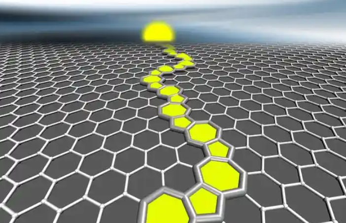
Chemical Vapor Deposition (CVD) graphene is a form of graphene synthesized by depositing carbon atoms onto a catalytic metal surface — usually copper or nickel — under high temperature and controlled atmosphere conditions.
The resulting film is typically a single layer (monolayer) or few layers of graphene with excellent uniformity and electrical conductivity.
Why CVD Graphene Matters
-
Large-area production: Unlike exfoliation or chemical reduction methods, CVD enables the growth of graphene films on scales suitable for industrial applications.
-
High structural quality: CVD-grown graphene exhibits minimal defects, maintaining the material’s intrinsic properties such as high carrier mobility, optical transparency, and mechanical strength.
-
Integration capability: The process allows direct or transferred integration onto various substrates — glass, polymers, silicon wafers, or metals — enabling wide functional use.
2. The CVD Graphene Production Process
The typical CVD graphene growth process involves several key steps: substrate preparation, hydrocarbon decomposition, graphene growth, and film cooling.
Step 1: Substrate Preparation
CVD graphene growth typically uses a metal catalyst, with copper (Cu) being the most common due to its low carbon solubility, which favors monolayer graphene formation.
Before growth, the copper foil is cleaned and annealed to remove surface oxides and impurities, improving crystal grain uniformity.
Step 2: Hydrocarbon Decomposition
A carbon-containing gas (usually methane, CH₄) is introduced into a high-temperature reactor (typically 900–1050°C) under a reducing atmosphere (e.g., hydrogen).
The methane decomposes into carbon atoms, which diffuse onto the copper surface and self-assemble into a graphene lattice.
Step 3: Graphene Growth Control
Growth time, temperature, and gas flow ratio determine the layer thickness and uniformity.
-
Shorter growth time → monolayer graphene
-
Longer growth time or higher methane concentration → few-layer graphene
Optimized parameters yield continuous monolayer films with high crystallinity and minimal defects.
Step 4: Cooling and Stabilization
After growth, the chamber is cooled under controlled conditions to prevent unwanted carbon precipitation or wrinkles.
The graphene-coated copper foil is now ready for transfer or direct application (depending on the target use).
3. Graphene Transfer Techniques
Since graphene grows on metal substrates, it often needs to be transferred onto an insulating or functional surface (e.g., glass, PET, or silicon oxide) for most applications.
This transfer process is critical to maintaining the film’s integrity and performance.
3.1 Wet Chemical Transfer (Polymer-Assisted)
The most common transfer method uses a polymer support layer such as PMMA (Polymethyl methacrylate):
-
A PMMA layer is spin-coated on the graphene surface.
-
The underlying copper substrate is etched away using an etchant (e.g., ammonium persulfate solution).
-
The graphene/PMMA film is floated onto water and then transferred to the target substrate.
-
PMMA is dissolved with acetone, leaving the graphene film behind.
✅ Advantages: Low cost and widely used
⚠️ Drawbacks: May leave polymer residue or cause wrinkles
3.2 Electrochemical Delamination
This “bubble transfer” technique uses electrolysis to separate graphene from the metal substrate:
-
The metal foil acts as a cathode, producing hydrogen bubbles that gently lift the graphene film.
-
The film is then transferred to the desired substrate with minimal contamination.
✅ Advantages: Cleaner surface and reusable metal substrate
⚠️ Drawbacks: Requires precise control to prevent film tears
3.3 Dry or Roll-to-Roll Transfer
For large-scale production, roll-to-roll (R2R) methods are used:
-
Graphene grown on copper foil is laminated to a target substrate using adhesive or thermal pressing.
-
The copper layer is subsequently etched or mechanically removed.
✅ Advantages: Suitable for mass production and flexible substrates
⚠️ Drawbacks: Equipment-intensive and less precise for small samples
4. Characterization and Quality Control
Ensuring the quality of CVD graphene films requires multiple characterization techniques to verify uniformity, defect density, and electronic properties.
| Technique | Purpose | Key Indicators |
|---|---|---|
| Raman Spectroscopy | Detects defect levels, layer number | ID/IG ratio, 2D peak shape |
| AFM (Atomic Force Microscopy) | Measures surface morphology | Roughness, wrinkles |
| SEM (Scanning Electron Microscopy) | Observes continuity and edges | Grain boundaries |
| Sheet Resistance Measurement | Evaluates electrical performance | < 500 Ω/sq for good monolayer |
| Optical Transmittance | Determines transparency | > 95% for single layer |
Quality control at each stage — from growth to transfer — is crucial for ensuring reproducibility and industrial reliability.
5. Industrial Applications of CVD Graphene Films
Thanks to their unique combination of high conductivity, optical transparency, and mechanical strength, CVD graphene films have found applications across several industries. Below are the most prominent sectors driving commercialization.
5.1 Transparent Conductive Films (TCFs)
CVD graphene serves as an alternative to indium tin oxide (ITO) in flexible electronics and displays.
Unlike brittle ITO, graphene films are flexible, bendable, and chemically stable, making them ideal for:
-
Flexible touch panels
-
OLED and LCD displays
-
Wearable electronics
Key Advantage: High transparency (~97%) with excellent surface conductivity and mechanical durability.
5.2 Energy Storage and Conversion
CVD graphene films are used as current collectors, electrodes, and protective coatings in advanced batteries and supercapacitors:
-
In lithium-ion and solid-state batteries, graphene films improve electron mobility and reduce internal resistance.
-
In fuel cells and hydrogen storage, graphene layers enhance catalytic activity and corrosion resistance.
Industrial Trend: Integration of graphene-coated foils or films in next-generation EV batteries and grid storage systems.
5.3 Sensors and Flexible Electronics
The extreme sensitivity of graphene to changes in charge, pressure, or chemical environment makes it ideal for sensor applications:
-
Gas sensors (detecting H₂, CO₂, NO₂, etc.)
-
Biosensors (for glucose or DNA detection)
-
Strain and pressure sensors in wearable devices
CVD graphene enables uniform sensor fabrication over large areas, ensuring stable and reproducible performance.
5.4 Thermal Management and Coatings
Graphene’s superior thermal conductivity (~5000 W/m·K) allows CVD films to act as heat spreaders in:
-
Electronic devices and LED modules
-
5G base station components
-
High-power semiconductors
Additionally, thin graphene coatings improve anti-corrosion, anti-static, and EMI shielding properties for industrial surfaces.
5.5 Optoelectronic and Photonic Devices
Because of its tunable bandgap and excellent optical absorption, CVD graphene is being explored in:
-
Photodetectors
-
Solar cells
-
Transparent electrodes in perovskite or organic PVs
When integrated with semiconductor wafers, it enables next-generation optoelectronic integration at nanoscale levels.
6. Challenges and Future Development
Despite remarkable progress, CVD graphene production still faces several technical challenges before full commercialization across all industries.
a. Transfer Process Complexity
Current transfer methods may introduce wrinkles, cracks, or polymer residues that degrade performance. Development of clean, scalable transfer or direct-growth techniques on dielectric substrates remains a priority.
b. Uniformity and Grain Boundaries
Achieving truly continuous, defect-free graphene over large areas is still difficult. Improvements in copper foil crystallinity and CVD reactor control are essential for industrial uniformity.
c. Cost and Throughput
Although costs have dropped significantly, CVD systems remain capital-intensive. Advances in roll-to-roll continuous growth and plasma-assisted CVD are expected to make graphene films more economical.
d. Integration Compatibility
For many applications (especially semiconductors and sensors), graphene must integrate with existing fabrication processes (e.g., CMOS lines). Progress in wafer-scale integration will unlock broader adoption.
7. The Future Outlook
The industrial landscape for CVD graphene films is rapidly maturing.
As transfer-free growth, large-area uniformity, and hybrid integration technologies advance, we can expect CVD graphene to transition from laboratory research to mainstream commercial applications in:
-
Smart wearables
-
Transparent and flexible displays
-
High-efficiency batteries
-
Advanced sensors and heat spreaders
With governments and companies worldwide investing heavily in graphene industrialization, CVD-grown films will continue to play a pivotal role in shaping the next generation of materials and devices.
CVD graphene film technology bridges the gap between scientific innovation and industrial application.
Through controlled synthesis, precise transfer, and growing integration into real-world systems, it delivers the unique combination of properties — conductivity, flexibility, and transparency — that no other material can match.
While challenges remain in scalability and cost, continuous R&D and process optimization are driving the industry closer to mass adoption. For manufacturers, integrators, and engineers, understanding CVD graphene’s production and transfer processes is essential to leveraging its full industrial potential.