
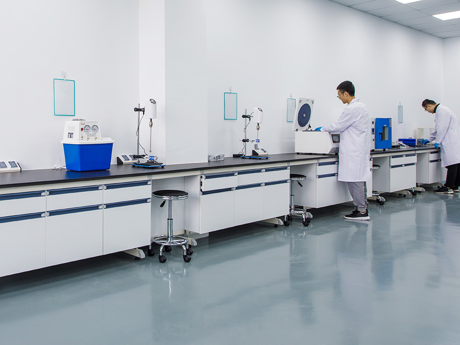
CNT-Based Field Emission Devices – Why Carbon Nanotubes Are Transforming Electron Sources
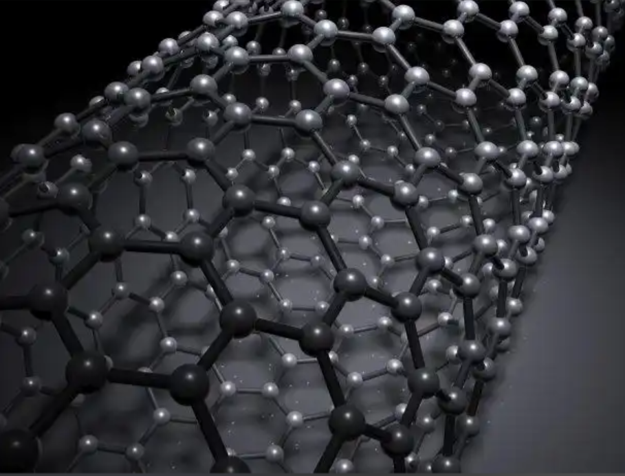
Field emission devices are the backbone of technologies that require highly efficient electron generation—ranging from next-generation displays and X-ray sources to vacuum microelectronics and space electronics. Carbon nanotubes (CNTs), with their exceptional electrical and structural properties, have emerged as one of the most promising field emission materials. Their high aspect ratio, excellent conductivity, and chemical stability make them ideal for low-voltage, high-current, and long-lifetime electron emission applications.
This article explains why CNTs are revolutionizing field emission technologies, how they are used, key design considerations, and the current challenges and opportunities.
1. Why CNTs Are Ideal for Field Emission
1.1 Ultra-High Aspect Ratio
CNTs feature tip radii as small as 1–10 nm, drastically enhancing local electric fields.
Result: electrons tunnel out at much lower voltages compared to metal emitters.
1.2 Superior Electrical Conductivity
Multi-wall CNTs (MWCNTs) and single-wall CNTs (SWCNTs) offer:
-
Low resistivity
-
High current-carrying capability
-
Stable emission even at elevated currents
This directly improves lifetime and energy efficiency.
1.3 Chemical and Thermal Stability
CNTs withstand:
-
High temperatures
-
Chemical corrosion
-
Plasma exposure
This allows operation in harsh or vacuum-based environments.
2. Key Application Areas
2.1 Field Emission Displays (FEDs)
CNTs enable:
-
Low-power cathode arrays
-
High brightness
-
Fast response time
-
Thin form factor
Many companies and research institutions are exploring CNT-FEDs as an alternative to LCD/OLED in high-brightness or ruggedized environments.
2.2 X-ray Sources
CNT emitters replace hot filaments with cold field emission cathodes.
Advantages:
-
Instant ON/OFF
-
Lower energy consumption
-
Higher resolution imaging (due to pulsed X-ray capability)
Used in medical imaging, security scanners, and portable diagnostic devices.
2.3 Vacuum Microelectronics
CNTs serve as efficient electron sources in:
-
Micro-vacuum transistors
-
Micro-pumping systems
-
High-frequency and high-power electronics
2.4 Space and Defense
CNT-based emitters support:
-
Compact electron sources for satellites
-
Radiation-resistant electronics
-
Electric propulsion research (neutralizers, ion sources)
3. How CNT-Based Field Emitters Are Fabricated
3.1 Direct Growth (CVD)
CNTs grown directly on the substrate ensure:
-
Strong adhesion
-
Uniform alignment
-
Longer lifetime
Typical substrates: Si, metal foils, metal-coated ceramics.
3.2 Screen Printing / Paste Coating
CNT ink/paste is printed onto electrodes.
Advantages:
-
Low cost
-
Compatible with large-area production
-
Suitable for flexible devices
3.3 Transfer of Vertically Aligned CNT Arrays
Used for precision devices requiring ultra-low turn-on voltage.
4. Performance Metrics You Should Care About
| Metric | Typical CNT Advantage |
|---|---|
| Turn-on field | 0.5–2 V/µm (very low) |
| Emission current density | >10 mA/cm² |
| Stability | Continuous operation over hundreds of hours |
| Uniformity | High due to aligned CNT structures |
CNTs outperform traditional materials such as molybdenum tips or doped silicon in nearly every aspect.
5. Challenges and Engineering Considerations
5.1 Emission Stability
CNT tips may degrade under high current.
Solution: surface functionalization, protective coatings, or optimized spacing.
5.2 Contact Resistance
Poor CNT–electrode contact limits long-term reliability.
Solution: metal catalyst layers, annealing, or direct growth.
5.3 Arcing & Breakdown
High-density CNT arrays may cause micro-arcing.
Solution: spacing optimization and passivation layers.
5.4 Uniformity Over Large Areas
Manufacturing consistent CNT emitters across large substrates remains challenging.
Screen-printable CNT pastes and vertically aligned growth techniques are being developed to resolve this.
6. Market Outlook
CNT-based electron emission technologies are rapidly moving from laboratories into real-world products:
-
Medical X-ray devices using CNT cathodes are already commercialized.
-
FED projects have been revived due to new interest in rugged, high-brightness displays.
-
Vacuum microelectronics is gaining momentum with the rise of radiation-hard and high-frequency applications.
-
Space and defense sectors are investing in CNT-based emission for compact electric propulsion and electron neutralizer systems.
Global market growth is forecasted to exceed 30% CAGR in the next decade as device integration and manufacturing costs improve.