

New Applications of Graphene Leading to Innovative Development Directions!
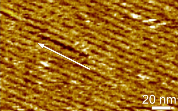
Although silk proteins have been used to design electronic products, their application has been limited due to the chaotic, pasta-like structure of silk fibers. Researchers from the Pacific Northwest National Laboratory (PNNL) have addressed this challenge. On September 18, they announced the achievement of a uniform two-dimensional (2D) layer of silk protein fragments on graphene—a carbon-based material known for its exceptional conductivity. The findings, titled “Two-dimensional silk,” were published in Scientific Advances. Atomic force microscopy images show the silk protein self-assembling uniformly on the graphene surface.
“These results provide a reproducible method for silk protein self-assembly, which is critical for designing and manufacturing silk-based electronic products,” said Chenyang Shi, the lead author of the study. “Notably, this system is non-toxic and water-based, which is vital for biocompatibility.” This combination of materials—silk-based graphene—can form sensitive, tunable transistors, which are highly sought after in the microelectronics industry for wearable and implantable health sensors. The PNNL team also sees potential for these transistors as key components in memory transistors or “memristors” within computational neural networks, enabling computers to mimic brain functions.
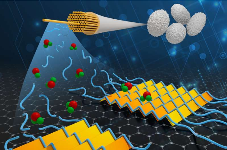
A single silk protein molecule, known as “fibroin” (in blue), deposits on a graphene surface surrounded by water (represented by green and red spheres) and grows into atomically precise two-dimensional (2D) sheets. Controlled deposition of silk fibers can produce a large quantity of biodegradable electronic devices. Image source: Mike Perkins | Pacific Northwest National Laboratory.
For centuries, silk production has remained a closely guarded secret in China, its reputation spreading along the famous Silk Road trade route to India, the Middle East, and Europe. By the Middle Ages, silk became a symbol of status and a coveted commodity in European markets. Even today, silk is associated with luxury and prestige, and its renowned qualities—elasticity, durability, and strength—make it suitable for advanced material applications.
“Many studies have used silk to modulate electronic signals, but the inherent disorder of silk proteins limits control,” said James De Yoreo, a researcher at PNNL and a professor of materials science and engineering and chemistry at the University of Washington. “So we thought, ‘What if we could create better interfaces?’” To achieve this, the team meticulously controlled reaction conditions to add individual silk fibers to a water-based system in a precise manner. Through controlled laboratory conditions, they achieved highly ordered 2D protein layers, with precisely aligned β-sheet structures—one of nature’s most common protein shapes.
Further imaging studies and complementary theoretical calculations indicate that the thin silk layer adopts a stable structure characteristic of natural silk. This nanoscale electronic structure (thinner than half a DNA strand) supports miniaturization in the bioelectronics sector. “This material is suitable for what we call field-effect transistors,” De Yoreo explained. “This means it acts as a transistor switch that can turn on or off based on signals. If you add antibodies, the transistor will switch states when target proteins bind.”
Researchers are planning to use this raw material and technology to manufacture their own artificial silk, incorporating functional proteins to enhance practicality and specificity. This study represents the first step in controlling the layering of silk in functional electronic components. Future research will focus on improving the stability and conductivity of silk integrated circuits and exploring the potential of silk in biodegradable electronic products to increase the application of green chemistry in electronic manufacturing.