Peking University in Science: Challenges and Opportunities for Graphene from Laboratory to Industrial Application!
On October 10, researcher Lin Li from Peking University and PhD student Zhao Yixuan published a review paper titled “Graphene, beyond lab benches” in the journal Science. The article focuses on the current application status and future development directions of graphene, a cutting-edge material, outside the laboratory. Since its discovery, graphene has attracted significant attention from both academia and industry due to its exceptional electrical, mechanical, and thermal properties. However, despite the immense potential demonstrated by high-quality graphene produced in the lab, large-scale production and application still face numerous challenges. The paper delves into the bottlenecks of graphene applications in electronic and optoelectronic devices and discusses the technical difficulties and solutions in the current industrialization process, while also forecasting graphene’s future prospects in industry and its potential revolutionary impact on existing technologies.
Original link: Science Article

Two decades after the discovery of graphene—a material composed of a single layer of carbon atoms arranged in a honeycomb structure—research on this remarkable material has evolved from the laboratory to large-scale production and commercial applications. Graphene is known for its wide array of extraordinary properties, including electrical conductivity that is up to 70% higher than that of copper, thermal conductivity at room temperature that is more than double that of graphite, and a strength 200 times greater than steel (with a weight only one-sixth that of steel). These properties make graphene and its derivatives ideal materials for various applications, including electronics, structural components, and biomedicine. However, broader industrial applications for graphene remain to be realized.
As described in the groundbreaking paper by Novoselov et al. in 2004, single-layer graphene sheets were produced by mechanically exfoliating highly oriented graphite using adhesive tape. This new material exhibited striking characteristics. Researchers observed a strong bipolar electric field effect, meaning that under applied gate voltages, it could switch between positive and negative charges. They also noted a high carrier mobility at room temperature, which is related to the speed at which electrons or holes move within the material. These characteristics indicate great potential for graphene in electronic applications. While mechanical exfoliation can produce defect-free graphene, it only yields small sheets measuring a few micrometers to hundreds of micrometers in size. As a result, early graphene research primarily focused on synthesizing high-quality single-layer or multilayer graphene in a continuous form on metal substrates using chemical vapor deposition (CVD) with carbon-containing precursors. However, limitations in production scale, significant quality variations between batches, and a lack of reliable methods to transfer graphene from one substrate to another have restricted the application of high-quality graphene films in electronic devices.
The initial focus of graphene research and commercialization centered on its derivatives, such as graphene nanoplatelets (particles composed of stacked two-dimensional sheets), graphene oxide with functional oxygen groups, and reduced graphene oxide (with the oxygen groups removed). Compared to defect-free graphene primarily produced by mechanical exfoliation with adhesive tape, these derivatives are easier to produce at scale, but often contain a large number of defects. Consequently, the potential applications of graphene have gradually shifted towards areas that can tolerate structural defects while still benefiting from the strength and lightweight properties of graphene derivatives, such as composites, coatings, and reinforcing materials. For example, graphene nanoplatelets have been used in anti-corrosion coatings, flame retardants, and electromagnetic shielding materials, with these applications approaching commercialization. Additionally, the conductivity, electrochemical stability, and excellent porous structure of graphene derivatives provide potential applications in energy storage and conversion devices.
In contrast, the industrial application of high-quality continuous graphene is still in its early stages. Electronic and optoelectronic devices require the synthesis of large-scale, uniform single-layer or multilayer graphene films with sufficiently high carrier mobility (typically above 10,000 cm²/Vs). Both laboratory and industrial sectors have worked to optimize the graphene growth process based on chemical vapor deposition (CVD) to reduce overall defect density and the number of grain boundaries and wrinkles, which hinder electrical transport. Furthermore, side reactions occur on the surface of graphene during large-scale production, such as the formation of amorphous carbon, which alters the inherent properties of graphene. Metal substrates (like copper foil) have been widely used to grow large-area single-layer graphene films. In surface-mediated growth mechanisms, the further multilayer growth is hindered due to reduced catalytic activity of the substrate covering the graphene, enabling precise control of film thickness. Currently, monocrystalline graphene films with reduced grain boundary density have only been achieved at the wafer level on metals. Moreover, depositing graphene films on non-metal substrates (such as semiconductors and insulators) is necessary for broader applications in electronic and photonic devices. Recently, CVD growth of graphene on insulating sapphire substrates has been demonstrated, marking a step forward in commercial electronic and optoelectronic applications. CVD-produced graphene has shown carrier mobilities exceeding 1,000,000 cm²/Vs, indicating that the gap between laboratory-grown graphene and defect-free graphene is closing. However, reported laboratory-scale devices are based on carefully selected areas within large-area graphene-coated substrates, resulting in significant differences between devices.

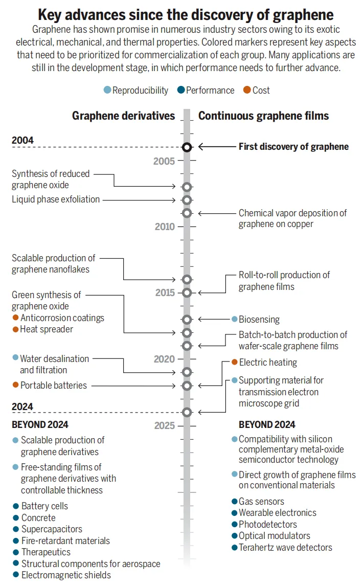
Key Advances in Graphene Since Its Discovery
Graphene has shown potential across multiple industrial sectors due to its extraordinary electrical, mechanical, and thermal properties. Colored markers represent key aspects requiring prioritization for commercialization. Many applications remain in development and require further performance enhancements.
From the perspective of electronic applications, the compatibility of CVD graphene with existing silicon-based complementary metal-oxide-semiconductor (CMOS) microfabrication facilities and technologies is crucial. Unfortunately, due to the formation of impurities such as carbides during the growth process, consistent growth of graphene on silicon/silica substrates is challenging. Additionally, amorphous silicon substrates cannot decompose carbon-containing precursors, leading to high defect densities in graphene films. The catalytic capability can be improved by introducing gaseous metal catalysts, but optimizing growth parameters for large-scale production of graphene on silicon substrates remains challenging.
One approach to address the silicon substrate issue is to first grow graphene on another substrate and then transfer it to the silicon surface. However, this method often results in cracks, wrinkles, folds, and other defects, leading to significant variations between devices and impacting production efficiency. These defects also alter the integration of dielectric materials with graphene. Dielectric materials are high-resistivity charge storage materials that determine the performance and operational stability of graphene-based electronic devices. Residual contaminants and pinholes (a type of defect in electronic devices) at the graphene-dielectric interface can reduce the carrier mobility of graphene films. As devices are miniaturized, even small defects can severely affect performance.
To suppress defects caused by transfer and improve dielectric integration, various strategies have been developed. Controlling peeling and layer pressure while avoiding the introduction of trace impurities helps reduce defects. Current silicon technologies also provide insights into how to create these processes. For example, using traditional wafer bonding techniques, graphene grown on copper substrates can be bonded to the desired substrate with an adhesive layer in between, followed by chemical etching to remove the copper layer. Another method promotes defect-free transfer of graphene by controlling the adhesion between the tape and graphene through ultraviolet light exposure. Additionally, van der Waals-layer dielectric materials like hexagonal boron nitride (hBN) and bismuth selenite (Bi₂SeO₅) can serve as support layers to assist in transfer and prevent interface contamination.
Nevertheless, these techniques have only been tested at the laboratory scale and require careful testing at the industrial scale. To avoid massive investments in large-scale production of graphene products, it is essential to develop processes compatible with existing manufacturing techniques. Furthermore, transferring large-area graphene films requires consistency in production capabilities. Integrating automated transfer processes, robotics, and machine designs into existing semiconductor facilities can enhance consistency. At the same time, developing methods for direct growth of graphene films on conventional substrate materials can bypass transfer-related issues, helping to accelerate commercialization. Thus, the commercialization of graphene-based products largely relies on collaboration between academia and industry.
A major challenge in the commercialization of graphene and its derivatives is the high production costs stemming from limited production volumes. Raw materials such as methane gas or graphite powder account for only a small fraction of total costs. In contrast, the design of equipment for large-scale batch production and processing of synthesized graphene constitutes most of the initial investment. Therefore, the industrial sector tends to favor high-profit applications that require less investment but can significantly enhance the performance of existing products. This has led to a faster commercialization of graphene derivatives for various structural components compared to high-quality graphene films for devices. For instance, the high production cost of graphene in transparent conductive films relative to traditional indium tin oxide (ITO) has hindered its adoption. Even graphene derivatives that have been commercialized or are on the verge of commercialization still need further cost reductions. The mainstream method for producing graphene nanoplatelet films is through filtration and layer-by-layer assembly utilizing electrostatic interactions; however, these methods are slow and unsuitable for large-scale production. Reducing costs without compromising performance is crucial for introducing graphene products to the market.

Differences in production methods across the industry lead to significant variations in the performance and characteristics of graphene products. This highlights the necessity of establishing standards for graphene and its derivatives. On this basis, the development of high-throughput characterization techniques is essential for measuring properties and filtering out non-compliant products. Optical characterization methods, such as ellipsometric contrast microscopy and terahertz time-domain spectroscopy, can quickly assess large-area graphene. However, some harmful structural defects can only be examined using advanced microscopy, which is often time-consuming. Automated characterization combined with machine learning and artificial intelligence can help overcome this limitation. For example, automated imaging and data analysis can identify features representing defects with minimal human intervention.
A significant gap remains between the needs of academia and industry, necessitating closer collaboration to bridge

