
Can Graphene Help Reduce Copper Dependency in Electronics?
Copper is one of the most important materials in modern electronics.
It is widely used in printed circuit boards (PCBs), semiconductor packaging, electrical interconnects, cables, connectors, heat dissipation components, and power distribution systems.
Its popularity comes from a combination of high electrical conductivity, good thermal conductivity, mechanical workability, relatively low cost, and a well-established global manufacturing supply chain.
However, the electronics industry is facing several evolving challenges.
As electronic devices become smaller, faster, more powerful, and more densely integrated, manufacturers are looking for alternative materials that can support improved electrical, thermal, and mechanical performance.
At the same time, copper supply chains face exposure to mining constraints, price fluctuations, geopolitical risks, and growing demand from electrification, renewable energy, electric vehicles, and data center infrastructure.
This raises an important question:
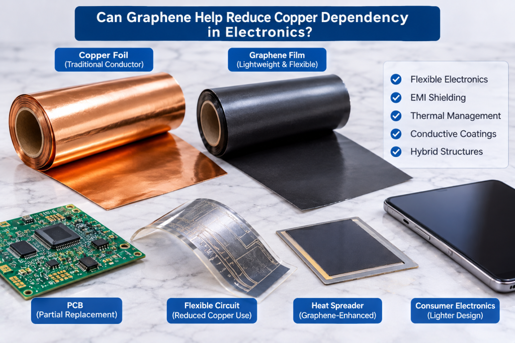
Can graphene help reduce copper dependency in electronics?
Graphene has exceptional intrinsic electrical and thermal properties, making it an attractive candidate for certain electronic applications.
However, replacing copper is not simply a matter of comparing the conductivity of two materials. Industrial adoption also depends on contact resistance, film quality, manufacturing compatibility, reliability, cost, and integration with existing electronic architectures.
In many applications, the most realistic opportunity may not be complete copper replacement, but rather using graphene to reduce copper consumption in selected functional layers or to develop hybrid graphene-copper structures.
This article explores where graphene may contribute to reducing copper dependency, where copper remains difficult to replace, and what technical challenges must be addressed before large-scale adoption becomes practical.
1. Why Is the Electronics Industry So Dependent on Copper?
Copper has become a foundational material in electronics because it offers a highly balanced combination of electrical, thermal, and manufacturing properties.
Its electrical conductivity is approximately 58 MS/m at room temperature for high-purity bulk copper, making it one of the most widely used engineering conductors.
Its advantages include:
- High electrical conductivity
- Good thermal conductivity
- Excellent ductility and formability
- Mature electroplating and etching processes
- Established PCB and semiconductor packaging technologies
- Broad industrial availability
- Extensive reliability and qualification experience
Copper is used in multiple electronic functions.
1.1 Electrical Interconnects
Copper is widely used for conducting electrical current between electronic components.
Examples include PCB traces, package substrates, connectors, lead frames, and internal device interconnections.
These applications require predictable resistance, stable interfaces, and reliable current-carrying performance.
1.2 Thermal Management
Copper is also used in heat spreaders, thermal plates, heat sinks, and other thermal management components.
Its high thermal conductivity allows heat to move efficiently away from localized hotspots.
This is particularly important in high-power electronics, semiconductor modules, and AI computing systems.
1.3 Electromagnetic Shielding
Copper is commonly used in shielding structures to reduce electromagnetic interference (EMI).
It provides high electrical conductivity and can be integrated into metal enclosures, conductive coatings, and shielding layers.
These functions create a substantial industrial dependence on copper.
However, not every electronic application requires a solid copper conductor. Some applications prioritize lightweight structures, flexibility, transparency, corrosion resistance, or multifunctional performance.
These are areas where graphene may offer alternative design possibilities.
2. Why Is Graphene Being Considered as an Alternative?
Graphene is a two-dimensional carbon material consisting of a single layer of carbon atoms arranged in a hexagonal lattice.
Its distinctive structure provides several properties that are attractive for electronic applications.
These include:
- High intrinsic carrier mobility under suitable conditions
- Excellent in-plane thermal conductivity
- High mechanical flexibility
- Low material density
- Potential optical transparency
- Chemical tunability through functionalization
- Compatibility with flexible and printed electronic architectures
However, intrinsic material properties should not be confused with the performance of a manufactured graphene film.
A theoretical graphene sheet and an industrial graphene coating are very different engineering products.
Commercial graphene films may contain grain boundaries, defects, wrinkles, transfer residues, interlayer contacts, and other structural imperfections.
These factors can significantly influence electrical and thermal performance.
The industrial opportunity therefore depends on whether graphene can deliver a measurable advantage in a specific electronic component, rather than whether its theoretical properties are impressive.
3. Application One: Transparent Conductive Films
One of the more established research directions for graphene in electronics is transparent conductive films.
Traditional transparent conductive electrodes often use indium tin oxide (ITO).
Although ITO is not copper, graphene may provide an alternative to certain transparent conductive materials and reduce dependence on brittle or supply-constrained materials in selected applications.
Potential applications include:
- Touch panels
- Flexible displays
- Transparent heaters
- Optical sensors
- Wearable electronics
- Flexible electronic devices
3.1 Why Graphene Is Attractive
Graphene combines electrical conductivity with optical transparency and mechanical flexibility.
This makes it interesting for applications where a conductive layer must remain functional while being bent or integrated into a flexible substrate.
Compared with brittle transparent conductive coatings, graphene-based films may offer advantages in certain flexible structures.
3.2 Industrial Challenges
The main challenge is achieving sufficiently low sheet resistance while maintaining high optical transparency.
Other important considerations include:
- Film continuity
- Grain boundary resistance
- Transfer damage
- Substrate adhesion
- Contact resistance
- Environmental stability
- Large-area manufacturing yield
For applications requiring high electrical conductivity, multilayer graphene may be considered, but additional layers can reduce transparency.
Graphene therefore offers application-specific opportunities rather than a universal replacement for transparent conductive materials.
4. Application Two: Printed and Flexible Electronics
Flexible electronics are another area where graphene may help reduce reliance on conventional metallic conductors.
Traditional copper circuits are highly effective, but their integration into flexible structures may require specialized fabrication, thin metal layers, or complex mechanical designs.
Graphene-based conductive inks and coatings offer alternative approaches for selected applications.
Potential uses include:
- Flexible sensors
- Printed electronic circuits
- Wearable devices
- Flexible heating elements
- Antistatic coatings
- Conductive textile structures
4.1 Graphene-Based Conductive Inks
Graphene nanoplatelets and other graphene derivatives can be incorporated into liquid formulations to create conductive inks.
After printing and drying, the graphene sheets form interconnected conductive pathways.
The resulting conductivity depends on several factors:
- Graphene material quality
- Sheet size and thickness
- Dispersion stability
- Binder selection
- Solid content
- Printing method
- Drying conditions
- Post-treatment
A major challenge is that the electrical resistance of printed graphene structures is often higher than that of bulk copper conductors.
For this reason, graphene inks may be more suitable for low-current, flexible, sensing, heating, or functional coating applications than for replacing conventional high-current copper wiring.
5. Application Three: Thermal Management in Electronics
Thermal management is becoming increasingly important as electronic power density continues to rise.
AI servers, high-performance computing systems, power electronics, and advanced semiconductor packages all generate substantial localized heat.
Copper is widely used for thermal management, but graphene offers interesting possibilities for lightweight thermal spreading and composite materials.
5.1 Graphene for Heat Spreading
Graphene has exceptionally high intrinsic in-plane thermal conductivity under suitable conditions.
In practical applications, graphene-based films may be designed to spread heat across a surface and reduce localized temperature concentration.
Potential applications include:
- Smartphone thermal management
- Semiconductor packaging
- Flexible electronic devices
- Battery thermal management
- LED modules
- High-density computing components
Graphene films may be especially attractive where low thickness, flexibility, and lightweight construction are important.
5.2 Graphene-Copper Hybrid Structures
Instead of replacing copper completely, graphene may be integrated into copper-based thermal structures.
Possible approaches include:
- Graphene-enhanced copper composites
- Graphene coatings on copper surfaces
- Graphene-containing thermal interface materials
- Hybrid graphene-metal heat spreaders
The goal may be to improve selected thermal or mechanical characteristics while retaining copper’s established manufacturing advantages.
However, the actual benefit depends on graphene distribution, interface quality, filler orientation, and manufacturing conditions.
The presence of graphene does not automatically improve the effective thermal conductivity of a copper composite.
Interfacial thermal resistance and structural defects must be carefully controlled.
6. Application Four: Electromagnetic Interference Shielding
Modern electronics require effective electromagnetic compatibility (EMC) and electromagnetic interference (EMI) control.
Copper shielding is widely used because of its high conductivity and mature processing technology.
Graphene-based materials may offer alternative shielding structures, particularly where lightweight, flexible, or multifunctional materials are needed.
Potential applications include:
- Flexible EMI shielding films
- Conductive polymer composites
- Lightweight electronic enclosures
- Shielding coatings
- Wearable electronic systems
- Flexible cables and device components
6.1 Why Graphene May Be Useful
Graphene can form interconnected conductive networks within polymer matrices.
These networks can contribute to electromagnetic shielding through reflection, absorption, and multiple internal scattering mechanisms.
The relative contribution of each mechanism depends on frequency, conductivity, thickness, material structure, and test configuration.
Graphene-based composites may therefore offer a way to integrate EMI shielding with mechanical flexibility and reduced material weight.
6.2 What Needs to Be Validated?
Important parameters include:
- Electrical conductivity
- Shielding effectiveness
- Frequency range
- Coating thickness
- Filler distribution
- Mechanical durability
- Adhesion
- Environmental stability
For applications with strict shielding requirements, performance must be compared with established copper-based solutions under identical test conditions.
7. Application Five: Conductive Coatings and Corrosion-Resistant Structures
Copper is not always the ideal choice for every conductive surface.
In certain environments, corrosion, oxidation, weight, or mechanical flexibility can create limitations.
Graphene-based coatings may provide additional functional properties when incorporated into suitable coating systems.
Potential applications include:
- Conductive protective coatings
- Corrosion-resistant electronic components
- Antistatic surfaces
- Functional metal coatings
- Conductive polymer layers
- Protective coatings for selected electronic assemblies
Graphene’s sheet-like structure may help create a barrier against the penetration of moisture and certain corrosive substances when it is well distributed in a suitable coating matrix.
However, graphene coatings require careful formulation.
Poor dispersion, defects, incomplete coverage, or unsuitable interfaces may reduce barrier performance.
In some metal systems, electrically conductive graphene in direct contact with the substrate may also create galvanic corrosion concerns under certain conditions.
Therefore, the coating architecture, substrate compatibility, and environmental exposure must be evaluated together.
8. Can Graphene Directly Replace Copper in PCB Manufacturing?
This is one of the most important questions for industrial adoption.
Copper remains the dominant material for PCB conductive traces because of its conductivity, processability, reliability, and established manufacturing infrastructure.
Graphene has attractive properties, but direct replacement faces several challenges.
8.1 Electrical Resistance
Commercial graphene films and printed graphene conductors often have higher effective resistance than conventional copper traces.
This can become a limitation in applications requiring high current density or low signal loss.
8.2 Contact Resistance
Electrical connections between graphene layers, metal terminals, and other electronic components can introduce additional resistance.
Even when graphene itself has excellent intrinsic conductivity, the complete connection structure may perform less effectively than expected.
8.3 Manufacturing Compatibility
PCB manufacturing involves established processes such as:
- Copper foil lamination
- Photolithography
- Chemical etching
- Electroplating
- Drilling and via formation
- Surface finishing
Graphene-based conductors must be compatible with these manufacturing steps or require alternative process architectures.
8.4 Reliability and Qualification
PCB applications require predictable performance over long service periods.
Manufacturers must evaluate:
- Thermal cycling
- Humidity resistance
- Adhesion
- Electrical stability
- Mechanical stress
- Electromigration-related reliability where relevant
- Production consistency
At present, graphene is more realistically viewed as a complementary material for selected PCB-related functions than as a general replacement for copper traces and interconnects.
9. The Most Practical Opportunity: Reducing Copper Dependency Through Hybrid Materials
The electronics industry does not necessarily need to eliminate copper to reduce its dependence on it.
A more realistic strategy is to identify functions where graphene can provide value alongside existing metallic materials.
Hybrid material systems may offer several advantages.
9.1 Graphene-Copper Composites
Graphene may be incorporated into copper-based structures to investigate improvements in selected properties.
Potential research directions include:
- Thermal management
- Mechanical reinforcement
- Wear resistance
- Electrical performance
- Lightweight functional structures
However, graphene dispersion in copper and the interface between graphene and the metal matrix are significant engineering challenges.
Poor interfacial contact may prevent the composite from achieving the expected performance.
9.2 Graphene-Enhanced Polymer Composites
Graphene can be incorporated into polymer matrices to produce lightweight conductive or thermally functional materials.
These composites may be suitable for:
- EMI shielding
- Antistatic components
- Conductive housings
- Thermal management structures
- Flexible electronic parts
In some applications, replacing a metal component with a graphene-filled polymer structure may reduce total copper consumption.
The feasibility depends on electrical requirements, mechanical strength, thermal performance, and manufacturing cost.
9.3 Graphene as a Functional Surface Layer
Another opportunity is using graphene as a thin functional coating rather than a bulk conductor.
For example, graphene-containing layers may provide conductive, protective, thermal, or barrier functions on existing components.
This approach may reduce the quantity of material required compared with replacing an entire copper component.
It also allows manufacturers to retain established metal structures while introducing new functionality.
10. What Prevents Large-Scale Industrial Adoption?
Despite its potential, graphene still faces several barriers before it can replace substantial quantities of copper in mainstream electronics.
10.1 Large-Area Material Quality
Large-area graphene production must maintain consistent film quality, electrical properties, and defect distribution.
Small variations can affect device performance and manufacturing yield.
10.2 Conductivity of Practical Graphene Products
The conductivity of a manufactured graphene structure is influenced by defects, grain boundaries, sheet-to-sheet contact, impurities, and processing conditions.
Intrinsic graphene properties cannot be used as a direct substitute for measured product performance.
10.3 Contact and Interface Engineering
Electrical and thermal interfaces can dominate the performance of practical devices.
Achieving reliable contact between graphene and metals, polymers, or semiconductor structures remains an important engineering challenge.
10.4 Manufacturing Cost
Graphene products must compete not only with copper prices but also with established manufacturing processes.
A technically attractive material may still be commercially unattractive if it requires expensive transfer, purification, post-treatment, or specialized equipment.
10.5 Long-Term Reliability
Industrial electronics require stable performance under real operating conditions.
Graphene-based structures must demonstrate durability under temperature cycling, humidity, mechanical stress, electrical loading, and other application-specific conditions.
11. How to Evaluate Graphene for Copper-Reduction Applications
A successful development program should begin with a clearly defined function rather than assuming that graphene is automatically a better conductor.
A practical evaluation process can include the following stages.
Stage 1: Identify the Copper-Dependent Function
Determine whether the objective is to reduce copper in:
- Electrical conductors
- Thermal spreaders
- EMI shielding layers
- Conductive coatings
- Flexible circuits
- Metal-based composite structures
Different functions require different material architectures.
Stage 2: Select the Appropriate Graphene Material
Potential material choices include:
- Graphene nanoplatelets
- Few-layer graphene
- Reduced graphene oxide
- CVD graphene films
- Functionalized graphene
- Graphene-based conductive dispersions
The selection should be based on the required electrical, thermal, mechanical, and processing characteristics.
Stage 3: Develop the Formulation or Hybrid Structure
Evaluate graphene loading, dispersion, binder compatibility, interface design, and manufacturing conditions.
For hybrid copper systems, the distribution and bonding of graphene within or on the metal structure are particularly important.
Stage 4: Compare Against a Copper Reference
Testing should use a conventional copper-based reference structure.
Relevant indicators may include:
- Electrical resistance
- Sheet resistance
- Thermal resistance
- Thermal conductivity
- EMI shielding effectiveness
- Adhesion
- Mechanical durability
- Environmental stability
Comparisons should be performed under equivalent dimensions, thicknesses, operating conditions, and measurement methods.
Stage 5: Validate Manufacturing Compatibility
A laboratory sample is not sufficient to establish industrial feasibility.
The material should be tested using relevant production processes, including coating, printing, lamination, curing, molding, or metal processing.
Stage 6: Evaluate Commercial Value
The final decision should consider more than material cost per kilogram.
Important factors include:
- Material consumption
- Manufacturing yield
- Processing cost
- Equipment investment
- Component performance
- Reliability
- Maintenance requirements
- Total cost of ownership
The objective is to determine whether graphene creates measurable economic or technical value compared with the existing copper solution.
Graphene has the potential to help reduce copper dependency in selected areas of the electronics industry.
Its most promising opportunities may include transparent conductive films, flexible electronics, EMI shielding, thermal management, conductive coatings, and hybrid metal-composite structures.
However, replacing copper in conventional PCB traces, high-current interconnects, and other demanding electrical applications remains challenging because of differences in practical conductivity, contact resistance, manufacturing compatibility, and long-term reliability.
The most realistic industrial strategy is not necessarily to replace copper completely.
Instead, manufacturers can investigate where graphene can reduce metal usage, introduce additional functionality, improve component design, or complement existing copper structures.
For graphene suppliers and electronics manufacturers, the key is to start with a specific engineering requirement, select an appropriate graphene product, and validate the complete component under realistic production and operating conditions.
Ultimately, graphene’s commercial value will depend not on theoretical properties alone, but on whether it can deliver measurable improvements at an acceptable manufacturing cost.
Frequently Asked Questions
1. Can graphene completely replace copper in electronics?
Not at present for most mainstream applications. Copper remains highly competitive in electrical conductivity, cost, manufacturing maturity, and reliability. Graphene is more promising in selected applications and hybrid structures.
2. Is graphene more electrically conductive than copper?
Ideal graphene has exceptional intrinsic electronic properties, but practical conductivity depends on film quality, defects, grain boundaries, contacts, and manufacturing conditions. Commercial graphene products should be compared with copper using measured component-level performance.
3. Can graphene replace copper in PCB traces?
Graphene is not currently a general drop-in replacement for conventional copper PCB traces. Higher effective resistance, contact engineering, via integration, manufacturing compatibility, and reliability qualification remain significant challenges.
4. Can graphene reduce copper use in thermal management?
Potentially, in selected heat-spreading films, composite structures, and thermal interface applications. However, the effective thermal performance of a manufactured graphene product must be measured rather than inferred from intrinsic graphene properties.
5. What electronic applications are most promising for graphene?
Potential application areas include flexible electronics, transparent conductive films, EMI shielding, conductive coatings, antistatic materials, and selected thermal management structures.
6. What is the advantage of graphene-copper hybrid materials?
Hybrid materials may combine copper’s established electrical and thermal performance with selected graphene-related properties. Their actual advantages depend on interface quality, graphene distribution, processing, and component-level testing.
7. What are the main barriers to graphene commercialization in electronics?
The main barriers include large-area material consistency, practical electrical conductivity, contact resistance, interface engineering, manufacturing compatibility, production cost, and long-term reliability.