20 Years of Graphene: Peking University’s Latest in Science!
Graphene, discovered 20 years ago, sparked a wave of excitement, drawing billions of dollars in research funding toward universities and startups striving to commercialize this atom-thin carbon layer. Recently, the so-called “wonder material” has seen a growing market—not only for monolayer graphene but also for graphene oxide (GO) and graphene nanoplatelets (GNP).
Graphene consists of a single layer of carbon atoms arranged in a honeycomb lattice. Research into this extraordinary material has evolved from the lab bench to large-scale production and commercial applications. Graphene is renowned for its remarkable properties, including electrical conductivity 70% higher than copper, thermal conductivity more than double that of pyrolytic graphite at room temperature, and strength 200 times that of steel while being only one-sixth its weight. These attributes make graphene and its derivatives highly suitable for applications in electronics, structural materials, and biomedicine. However, broader industrial adoption has yet to materialize.

The journey began with a groundbreaking paper in 2004 by Novoselov et al., where they used adhesive tape to mechanically exfoliate highly oriented pyrolytic graphite, producing monolayer graphene sheets. This new material revealed fascinating properties. The researchers observed a strong bipolar electric field effect, which allowed the switching between positive and negative charge carriers by applying gate voltage. Additionally, they noted high room-temperature carrier mobility, reflecting how quickly electrons or holes could travel through the material. These traits highlighted graphene’s potential for electronic applications.
Though mechanical exfoliation yielded pure graphene, it produced only small flakes, typically ranging from tens to hundreds of microns. Early research thus focused on synthesizing continuous high-quality monolayer or multilayer graphene using chemical vapor deposition (CVD) on metal substrates. However, scaling up production proved challenging. Quality inconsistencies across batches and the lack of reliable methods to transfer graphene between substrates have slowed the adoption of high-quality graphene films in electronic devices.
Bridging the Gap Between Research and Industry: Peking University Reflects on 20 Years of Graphene
Professor Lin Li from Peking University and his team have reviewed the progress of graphene over the past two decades, pointing out that a significant gap remains between academic research and industrial needs. They highlight the necessity for stronger collaboration to close this gap and promote real-world applications.
The article emphasizes the importance of developing a comprehensive standardization system with performance-based classifications tailored to specific applications. This framework would guide products toward relevant markets by defining the essential properties for each function and their corresponding measurement methods. Such standards should be jointly drafted by researchers, manufacturers, and end-user companies to ensure alignment across the supply chain.

The review, titled “Graphene, Beyond Lab Benches,” was published in Science to mark the 20th anniversary of graphene’s discovery and celebrate its journey from the lab to potential commercialization.
Key Advances in Graphene: Challenges and Solutions in Commercialization

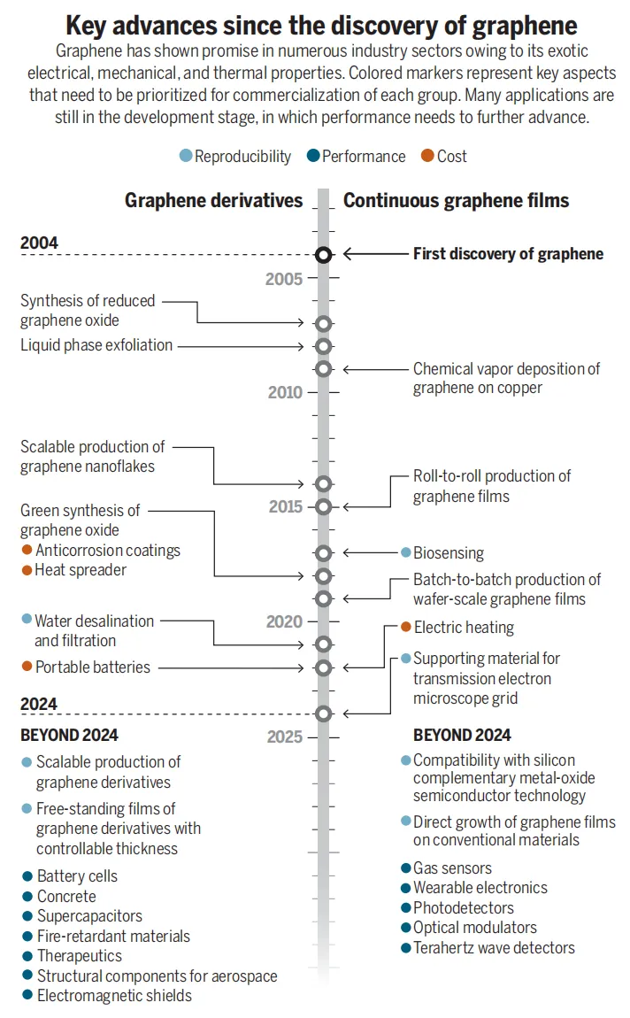
Figure 1: Key Progress Since the Discovery of Graphene
From the perspective of electronic applications, the compatibility of graphene with existing microfabrication technologies is crucial, especially for silicon-based Complementary Metal-Oxide-Semiconductor (CMOS) systems. However, achieving conformal graphene growth on silicon/silicon dioxide substrates has proven difficult due to the formation of impurities such as carbides during the growth process. Additionally, amorphous silicon substrates cannot efficiently decompose carbon precursors, leading to graphene films with high defect densities.
Introducing vapor-phase metal catalysts has improved catalytic efficiency, but optimizing growth parameters for large-scale graphene production on silicon remains challenging. One potential solution is to grow graphene on separate substrates and then transfer it onto silicon. However, this transfer process often introduces defects like cracks, wrinkles, or folds, which cause performance variability between devices and reduce production yields.
These imperfections also disrupt the integration of dielectric materials with graphene. Since dielectric materials store charge with high resistivity, they play a critical role in determining the performance and stability of graphene-based electronic devices. Contamination from transfer-related residues and electron defects (holes) at the graphene-dielectric interface further deteriorate carrier mobility. As devices continue to shrink, even minor defects can significantly impair performance.
Although these technologies have shown promise in lab settings, scaling them up for industrial use remains a significant challenge. The commercialization of graphene relies heavily on collaborations between academia and industry. One of the primary obstacles to commercialization is the high production cost. While raw materials like methane gas or graphite powder account for only a small fraction of total expenses, most of the initial investment goes into designing equipment for mass production and processing of synthetic graphene.
As a result, industries tend to focus on high-margin applications that deliver noticeable performance improvements with minimal investment, rather than pursuing high-quality graphene films for electronic devices. Variations in production methods also cause significant differences in the performance of graphene products. This underscores the need for well-defined standards for graphene and its derivatives. Developing high-throughput characterization techniques will be essential to measure product properties and filter out those that do not meet industry standards.
Original Source:
Yixuan Zhao, Li Lin, Graphene, beyond lab benches, Science, https://www.science.org/doi/10.1126/science.ads4149

